
Building a Scanning PALM Microscope
Construction
Over the course of the semester, the microscope took shape.
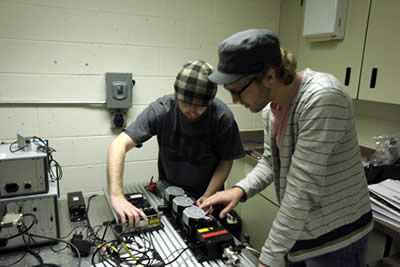
Figure 1: Alek (left) and Tyler (right) installing the lasers and collimating them along a common path for the excitation path of the optical system.
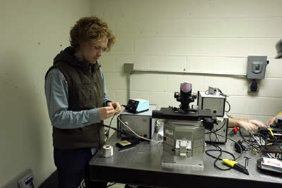
Figure 2: Jason about to fix a broken cable used to move the objectives on the iMic body (which is sitting in the center of the table).
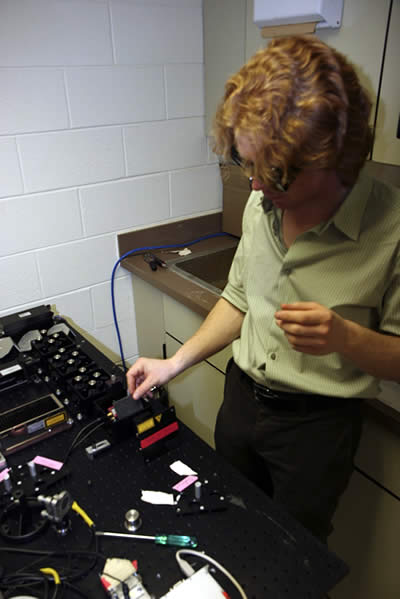
Figure 3: Jason checking the shutter control on the laser system.
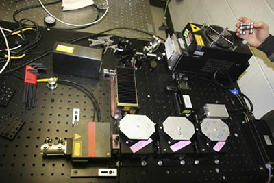
Figure 4: Combining three lasers into one optical path.
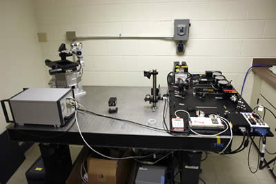
Figure 5: Rearrangement of the optical table to make space for the needed components.
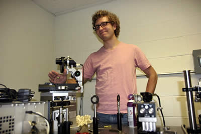
Figure 6: Tyler showing the light bouncing off of his hand, proof of the light going through the microscope body, the excitation path is nearly done!
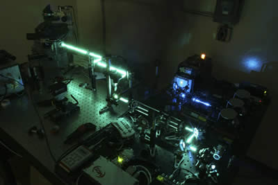
Figure 7: 30 second exposure photograph of the system with the excitation path setup and the lasers going into the microscope body. Tyler is the blurred image in the background; he is waving his fingers with a reflective coating on them in and out of the laser beam, thus showing the beam path as it reflected off of his fingers and into the camera.

Figure 8: Starting to work on the detection path. The old monitor is used to help determine the focal plane of the system.
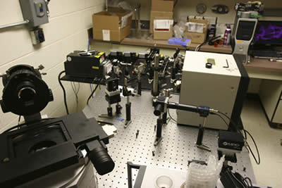
Figure 9: System from a different angle. One can see the scanning mirror (black mirror on two legs just left-of-center); a scanning mirror is central to any confocal system. Most systems use two scanning mirrors, one for a horizontal movement, and one mirror for vertical movement. This system uses a mirror that has simultaneous movement in both the horizontal and vertical direction.
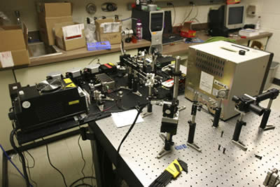
Figure 10: Here one can see a closer shot of the scanning mirror.
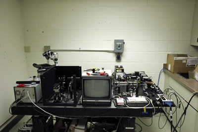
Figure 11: Finalized system. The detection path has been setup, with an avalanche photo-diode (APD) as the photon counter for the system.
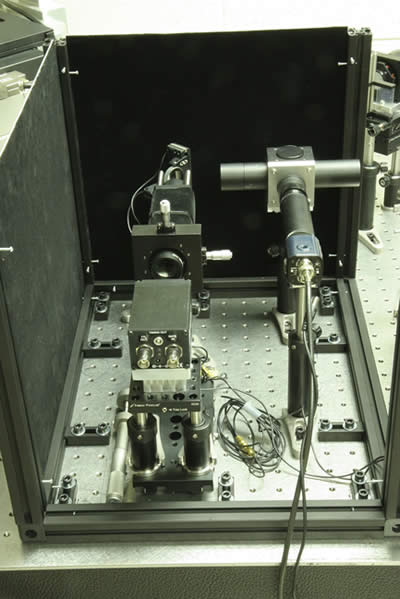
Figure 12: Close-up of the detection path.
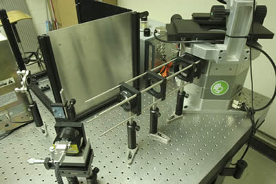
Figure 13: Close-up o the scanning mirror (bottom of photo) and the scan and tube lenses in place before the iMic microscope body.
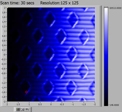
Figure 14: First image off of the constructed microscope. This is a silicon grid used for calibration purposes. Each square is 5 microns wide, and they have a spacing of 5 microns between them.